6502 RAM/ROM Expansion construction

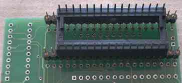
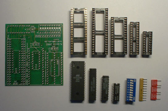
If you ordered a kit, you should have gotten all the components on this picture. If you ordered just the PCB, you'll have to get these or similar components yourself (see the main page for a parts list). Note that the GAL is not included in the kit and therefore is not shown here. The same goes for the 6502 CPU!

kit1


Disk drive special notes

The disk drives turned out to have a very special memory map that can lead to problems with an unmodified 6502 expansion board. If you want to make use of the expansion RAM at $2000-$7fff, a small hardware patch has to be applied. All other functions work without the patch as well: Expansion RAM at $0000-$07ff and $8000-$9fff, and the Flash ROM at $8000-$ffff. The patch has to be undone if the board is to be used in a PET or VIC-20 computer. This is as simple as soldering one wire end to another terminal of the GAL socket. A small switch could also be added.

The fix involves cutting the connection of the A15 signal between the expansion board and the 6502 socket adaptor, and applying a modified A15 signal from the GAL chip. The following steps are needed:

Installing the patch:
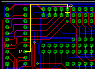
1. Cut the two copper traces (on both the top and bottom side of the board!) between  pin 25 of the CPU socket IC1 and pin 25 of the CPU socket adaptor CN1.
2. Solder a wire from pin 25 of the CPU socket adaptor CN1 to pin 18 of the GAL socket IC4.
Uninstalling the patch:
1. Disconnect the wire from pin 18 of the GAL socket IC4 and install it to pin 4 of the GAL socket IC4.

1541 pcb fix
A picture that shows the changes from the bottom side of the PCB.

Patch for Version 1.1 PCBs:
There is now a jumper for selecting the patch mode. You can install a jumper header here, or a simple wire link if you don't plan to change the mode often.

For PET and VIC usage, make a link between the left and middle pads, for 15xx (disk drive) usage make a link between the middle and right pads.

patch jumper setting
the new Jumper field shown from the top side of the PCB.

General instructions

Assembling the device includes a few tricky steps, especially installing the socket adaptor. The instructions below are not the only way to do it, but it is what I thought is easiest and most straight forward.

Please read through the whole set of instructions first before you solder anything. It's also a good idea to do a simulation run and insert the components without actually soldering them, so you can see if your end results matches the pictures you see on these pages. If not, you can still undo everything and start over without having to desolder everything!

1a
I'm now using and supplying another type of socket adaptors, this makes the soldering of the 40 pin socket much easier, but requires an extra step to keep the socket adaptor rows aligned. Simply put the two rows into a socket for this, solder the four corner pins to keep the rows in place (I do this from the bottom side so the adaptor rows don't get misaligned), and then remove the socket again. The remaining pins should be soldered from the top side.

I find it easier to install these adaptor rows as the first step, before installing IC5. Please also read the explanations under step 2 before soldering anything!
sil adaptor
1b
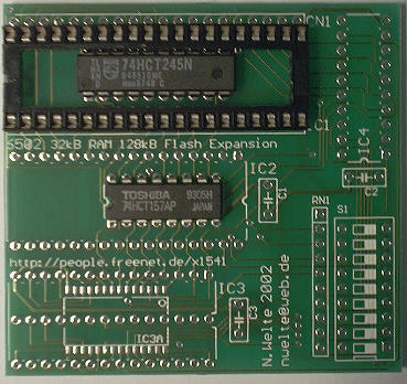
Cut out the central stabilizer bar from the 40 and 32pin socket. I use a small wire cutter for this. In the 40 pin socket, remove the remaining plastic carefully with a sharp knife, because the 74HCT245 fits very tightly inside the socket. Now insert the 74HCT245 into the board, but do not solder it yet. Also insert the 40 pin socket, you might have to press a little bit to get it into place. Now turn the board around and solder the 74HCT245 into the place it has been put now (it might not be centered in its holes). You can also solder in the 74HCT157 now. Do not solder the 40pin socket yet!

At this point, you can also solder the SMD-SRAM at IC3a if you decided to use it instead of the Cache-SRAM.
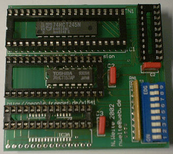
kit2
2.
If you already installed the socket adaptors in step 1a, please go on with step3.

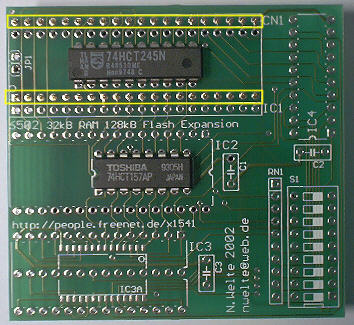
Now the socket adaptor will be installed from the lower side of the board. The pins have a thick and a thin end, the thick (and probably shorter) end will have to be soldered into the board. If you insert the adaptor, you will see that it can't be inserted completely because of the 40pin socket, but the pins can stick out of the top side enough to be soldered from there (This is the same as the high-profile version on the 2364 adaptor page, look there for pictures). So remove the 40pin socket now and solder the socket adaptor from the top side (see the yellow markers). It's a good idea to solder the four corner pins first and check the alignment of the socket and if the 40 pin socket can be inserted far enough. When you have completed soldering the socket adaptor, insert the 40 pin socket again and finally solder it into place. Some pins may be hard to reach, but it's possible without melting the socket. Believe me :-)

kit3
3.
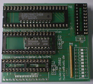
The hardest part is already done, the rest is easy: the remaining sockets must be installed now. This is pretty straightforward, just insert and solder them. The resistor package will also be soldered now, pay attention that Pin 1 is aligned correctly. kit4
4.
As the last soldering step, the DIP switch and the capacitors will be soldered in. After this, control the lower side of the PCBs carefully for short circuits that are caused by using too much solder. kit5
5.
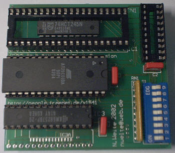
Now insert the remaining components into the sockets: The AT29C010A Flash-ROM and the 256kbit SRAM. You can also insert the GAL and the 6502 CPU now. Congratulations, the device is ready for use now! kit6

Troubleshooting

If your device isn't working as it should, then there is some help here. Of course, you should check for short circuits or forgotten solder joints first, but there is also a special procedure that you can use to do a basic test:

- remove all socketed components, i.e. the GAL, the RAM, the FlashROM.
- set all the DIP switches to the OFF position
- now put a wire into the GAL socket, connecting pins 10 and 16. This will enable the 74HCT245 bus transceiver.
- if you have installed the 1541 patch wire, also connect pins 4 and 18. This will connect the A15 line of the CPU.
- now install the board into the CPU socket and plug the CPU into the board. Turn on the device, it should work now.

If this test was successful, it means the board has no short circuits, and the 74HCT245 is working. Now you can remove the test wires and install the GAL chip instead. If the board stops working, then there is a problem with this chip, or with the socket connections.

Next, install the Flash chip and try the board again. You should be able to flash a ROM and then run your device from the Flash chip. If this doesn't work, be sure to try all four possible banks. Maybe there is only a problem with the 74HCT157 chip, which is connected to the banking lines. If you have the possibility, you can program an EPROM accordingly and use this instead of the Flash chip and see if at least the reading works. A 27(C)256 or 27(C)512 can be used, probably the 27(C)010, too.

Contact

If you have questions about this project,  you can mail me: please visit my contact page.