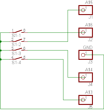
28 pin (for 23128/23256)
(depends on EPROM type used)
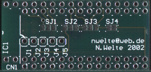
The PCBs are double sided and require some skills to be built. The layout files were created with Cadsoft's Freeware version of Eagle 4.09 and can be downloaded here. The file contains layouts and schematics for other projects, too. You can also buy the PCBs from me, just visit the order page.
The following components are needed:
| IC1 | Flash-ROM or EPROM | 27C64-27C512, 29C256-29C010 and pin compatible devices (so
27xxx, 28Cxxx and 29Fxxx should work fine) |
 |
| CN1 | precision socket adaptor | 24 pin (for 2364) or 28 pin (for 23128/23256) |
|
| R1,2,4,5 | SMD resistors | 4.7kOhm, 0805 package (optional) | |
| S1,2,4,5 |
switch |
(optional) | |
| IC socket |
32pin or 28pin IC socket (depends on EPROM type used) |
||
For details on assembling the device, please refer to the construction page. Before you start soldering
parts, you have to configure the board's
jumpers!
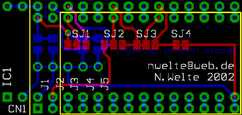
| Use of 28 pin EPROMs or Flash-ROMs in a
machine with very limited space: In this case you can cut off the extra
board space with a small hacksaw, but be careful not to damage the part
of the board you still need. The edge to cut is shown with the yellow
line. This picture also shows the place where a 24 pin socket adaptor has to be installed, if you want to replace 2364 ROMs. Installation in a 24pin 2364 socket does not need any special changes to the board, except the adjustments needed for the EPROM bank selection (see below), because the board comes preconfigured for 2364 mode. |
 |
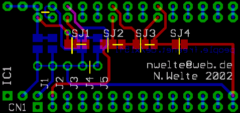
| If you want to install the adaptor in a 23128 socket (usually found in the
C64E board and the C128 and (plastic case) C128D machines), perform the
following changes: cut the traces that connect the pads of SJ1 to SJ4,
then close the other pads of SJ1 to SJ3 with a blob of solder and a
short piece of wire, if needed. Also cut the two traces on the bottom
side of the board, as shown in the picture. These traces are located
between J4 and J5, and between pins 27 and 28 of the DIP 28 adaptor
socket. Do not install a resistor to
R5! If you want to use an EPROM, and/or you want to make use of the extra memory banks, you have to cut the traces between J1, J2, J3 and J4 as well, and install the three resistors that correspond to J1, J2 and J4. Refer to the picture below for details. |
 |
| If you want to install the adaptor in a 23256 socket (usually found in
the (metal case) C128DCR machine only), perform the following
changes: cut the traces that connect the pads of SJ1 to SJ4, then close
the other pads of SJ1 to SJ3 with a blob of solder and a short piece of
wire, if needed. Also cut the two traces on the bottom side of the
board, as shown in the picture. These traces are located between J3 and
J4, and J4 and J5. Do not install
resistors to R4 and R5! If you want to use an EPROM, and/or you want to make use of the extra memory banks, you have to cut the traces between J1, J2 and J3 as well, and install the two resistors that correspond to J1 and J2. Refer to the pictures below for details. |
 |
| Flash/EPROM
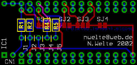
size and banking adjustments: Since a 29C010 can hold 16 times the contents of a 2364 ROM, many different ROM images can be stored in it. To select one of these images, the extra address lines have to be set to the desired levels. In the standard configuration of the adaptor all lines are grounded with the tiny traces between the solder joints J1 to J5, so bank 0 of the Flash chip is selected. If you need the other banks, these traces have to be cut open (yellow lines), pull-up resistors must be installed on the bottom side of the board in the space shown by the yellow rectangles. See the construction page and the next chapter for details. |
 |
| address line |
chip size |
chip type |
| A16 |
1Mbit |
29C010 |
| A15 |
512kbit |
27C512/29C512 |
| A14 |
256kbit |
27C256/29C256 |
| A13 |
128kbit |
27C128 |
| banks |
address line |
jumper |
resistor | cut trace | notes |
| 16 |
A16 |
J2 |
R2 |
J2-J3 |
requires A15, too! |
| 8 |
A15 |
J1 |
R1 |
J1-J2 |
required on 2764-27256 |
| 4 |
A14 |
J4 |
R4 |
J3-J4 |
requires A13, too! required on 2764-27128 |
| 2 |
A13 |
J5 |
R5 |
J4-J5 |
| banks |
address line |
jumper |
resistor | cut trace | notes |
| 8 |
A16 |
J2 |
R2 |
J2-J3 |
requires A15, too! |
| 4 |
A15 |
J1 |
R1 |
J1-J2 |
required on 27128-27256 |
| 2 |
A14 |
J4 |
R4 |
J3-J4 |
requires A13, too! required on 27128 |
| banks |
address line |
jumper |
resistor | cut trace | notes |
| 4 |
A16 |
J2 |
R2 |
J2-J3 |
requires A15, too! |
| 2 |
A15 |
J1 |
R1 |
J1-J2 |
required on 27256
|
