

The PCBs are double sided and require some skills to be built. The layout files were created with Cadsoft's Freeware version of Eagle 4.09 and can be downloaded here. The file contains layouts and schematics for other projects, too. You can also buy the PCBs from me, just visit the order page.
The following components are needed for the 6550 RAM adaptor:
| IC2 | 74LS00 SMD | (combine R/W with Phi2) |
| IC1 | SRAM | 6116, 6164 or 61256 |
| CN1 |
precision socket adaptor | 22 pin |
| CN2 |
precision socket adaptor | 22 pin |
| IC1 | EPROM | 2716-27C512 |
| CN1 |
precision socket adaptor |
28 pin |
| R1-R3 |
4.7kOhm resistors 0805 package |
(optional) |
The 6540 adaptor can optionally be equipped with some switches and
pull-up resistors to allow the selection of different character ROM
images. You can use this to hold both the BASIC1 and BASIC2 versions of
the character set and maybe sets of national characters. Up to eight
different images can be selected, depending on the size of the EPROM
you
use. The jumper wire connectors are mapped as follows:
| jumper |
signal |
banks |
EPROM type |
| J1 |
A11 |
2 |
2732 and above |
| J2 |
A12 |
4 |
2764 and above |
| J3 |
A13 |
8 |
27128 and above |
| J4 | ground connection |
Note that you have to cut the trace between the solder pads of the
resistor and install the resistor if you want to make use of the extra
character ROM banks, otherwise you will produce a short circuit if you
close the switch between J1-3 and J4! If you need only 2 or 4 banks,
but
have a larger EPROM, just leave the resistor pad(s) corresponding to
the
extra address line(s) alone. Address lines A14 and A15 as present on
27256 and 27512 EPROMs are always connected to logical high. Remember
this when burning the ROM images into the EPROM.
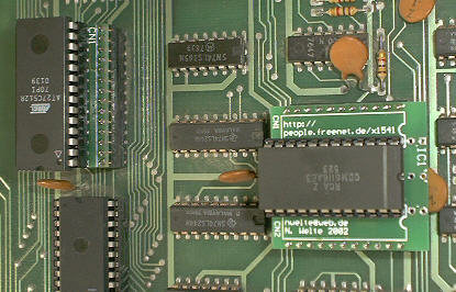
Here are some pictures of the PCB layout and the adaptors themselves:
 |
 |
 |
| The 6540 adaptor | The dual 6550 adaptor | final adaptors in action |