The A570 2MB RAM expansion

The A570 has two expansion slots: one external slot for an optional
SCSI adaptor and an internal one for a 2MB RAM expansion. Commodore
didn't make expansions for either one, but there are some third-party
SCSI adaptors to plug into the external slot. It's not sure if a RAM
expansion was ever produced, so I decided to make my own one.
The biggest problem with designing the expansion was that the
schematics for the A570 were never released by Commodore. The best I
could get were schematics for the CDTV and the A590. The CDTV is
very similar to the A570, but it is older and less integrated, and it
does not have a port for a memory expansion at all. The A590 is a
completely different device, but based on the same DMAC chip and it
does
have the RAM expansion. With this information and some measurements
with
an Ohm meter I could figure out all signals on the expansion connector
except six, which are connected to the XC2064 programmable logic chip.
With the help of an oscilloscope I could identify RAS and CAS, but not
the other four signals. So I decided to make a prototype that has a
patch field for these signals. I already learnt that the A570 supports
1MBit type DRAMs (not 256kbit like the A590!) and it has the
multiplexing circuit already on the mainboard. So the memory board just
needs to have the memory chips themselves.
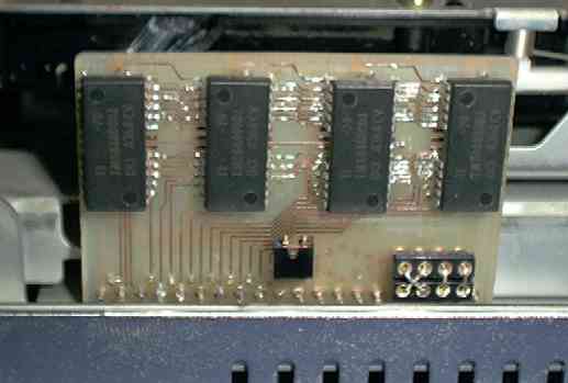
Due to the very limited space inside the A570 I had to use 1M x 4 RAMs
that I got from an old 4MB PS/2 SIMM. In the picture the patch field
and
the jumper for selecting the expansion are visible as well:
The expansion works perfectly and passes the RAM test program that is
supplied on the A2091 test disk. This is yet another device with the
same DMAC chip. There are 24 possible combinations to configure the
patch field (4 x 3 x 2 x 1) and I had to test them all! Most of them
lead to an error code when starting the Amiga, some manage to get it
started, but then there is no expansion RAM. Only one is valid, and
with
this the following pinout diagram can be made:
signal
|
pin
|
pin
|
signal
|
GND
|
1
|
2
|
GND
|
D0
|
3
|
4
|
D1
|
D2
|
5
|
6
|
D3
|
D4
|
7
|
8
|
D5
|
D6
|
9
|
10
|
D7
|
D8
|
11
|
12
|
D9
|
D10
|
13
|
14
|
D11
|
D12
|
15
|
16
|
D13
|
D14
|
17
|
18
|
D15
|
RAMSZ
|
19
|
20
|
GND
|
Vcc
|
21
|
22
|
Vcc
|
MA0
|
23
|
24
|
MA1
|
MA2
|
25
|
26
|
MA3
|
MA4
|
27
|
28
|
MA5
|
MA6
|
29
|
30
|
MA7
|
MA8
|
31
|
32
|
MA9
|
/WEL
|
33
|
34
|
/OEL
|
RAS
|
35
|
36
|
CAS
|
/OEH
|
37
|
38
|
/WEH
|
GND
|
39
|
40
|
GND
|
Contact
If you have questions about this project, you can mail me: please
visit my contact page.